Engineers are available to assist.


From fast modifications to stock optics to custom designs, we can help you take your optical system from design to prototype to volume production. Contact us to get started today.
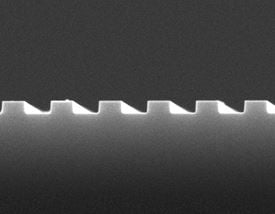
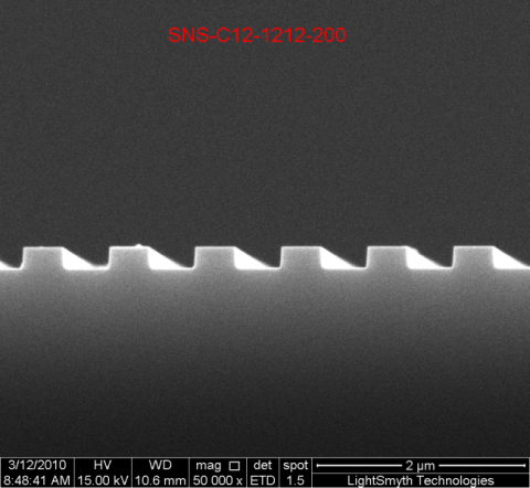
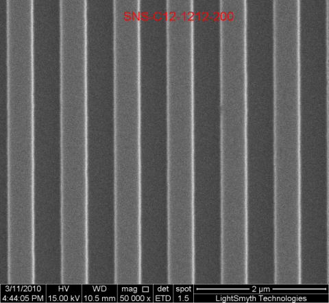
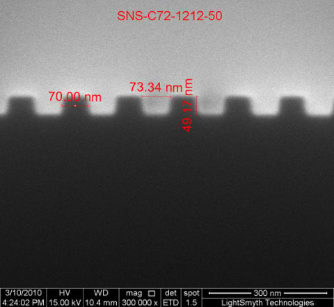
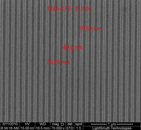
Coherent® LightSmyth™ Nanopattern Silicon Stamps consist of nanoscale-textured surfaces patterned on single-crystal silicon substrates. Through reactive ion etching, linear grooves with a trapezoidal cross-section are etched into the substrate surface, resembling conventional gratings. The etching process enables different period and depth specifications for these grooves, as well as more complex patterns such as lattices. Coherent® LightSmyth™ Nanopattern Silicon Stamps are ideal for nanophotonics research applications in the fields of optics and photonics, biology, chemistry, nanoimprinting, and microfluidics.
Note: II-VI Incorporated is now Coherent Corp.


or view regional numbers
QUOTE TOOL
enter stock numbers to begin
Copyright 2023, Edmund Optics Inc., 18 Woodlands Loop #04-00, Singapore 738100
California Consumer Privacy Act (CCPA): Do Not Sell or Share My Personal Information
California Transparency in Supply Chains Act